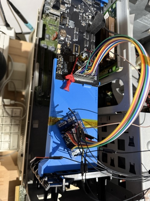
After several weeks of design work, I finally received the first WonderMCA prototype PCB. I’ve been using JLCPCB for months now, and they consistently deliver: the quality is excellent and the path from design to physical board is remarkably smooth.
The First Milestone: Four Basic Transfers
My first milestone was to get the WonderMCA (WM) handling the four fundamental MCA bus transfer types:
- MEMR — Memory Read
- MEMW — Memory Write
- IOR — I/O Read
- IOW — I/O Write
Per the MCA specification, these transfers are encoded on the bus as follows:
| Transfer | M/IO | S0 | S1 |
|---|---|---|---|
| MEMR | 1 | 1 | 0 |
| MEMW | 1 | 0 | 1 |
| IOR | 0 | 1 | 0 |
| IOW | 0 | 0 | 1 |
I started my experimentation on the PS/2 model 55 for no specific reason, and it was a good choice to start and I discover also very quickly the cliff in front of me.
Memory cycles (MEMR/MEMW) must complete in 200 ns; I/O cycles (IOR/IOW) get 300 ns. 200 ns is incredibly short — and as I would later discover, the real bus timing is even tighter than I had initially appreciated.
Within that 200 ns window, the card must:
- Poll for a new bus cycle
- Capture the high address (upper 12 bits)
- Switch the multiplexer to the low-address bank
- Capture the low address (lower 12 bits)
- Switch the multiplexer to data mode (read or write)
- Read or write the data byte
- Switch the multiplexer back to high-address mode
Choosing the MCU and Clocking It Hard
The RP2350B (which I’ll just call the “RP” from here on) runs at 150 MHz by default — that’s 6.6 ns per CPU cycle, giving roughly 30 cycles to do everything above, with zero margin.
Fortunately, the RP2350B can be safely overclocked to 360 MHz, dropping the cycle time to 2.8 ns and giving me real breathing room. To make that work reliably, the core voltage and the flash clock divider both need to be adjusted.
The RP2350B is a dual-core ARM-based MCU with PIO (Programmable I/O) blocks. My initial architecture was:
- Core 0 — UART debugging
- Core 1 — MCA bus processing (the time-critical path)
- Inter-core FIFO — for non-blocking messages between the two cores
There are two multiplexer control signals on the board: one to switch between Data and Address modes, and one to switch between the high and low halves of the address bus:
| Mux Mode | A_AB | D_OE |
|---|---|---|
| Addr Low | 0 | 1 |
| Addr High | 1 | 1 |
| Data | — | 0 |
Cycle-Accurate Bus Capture
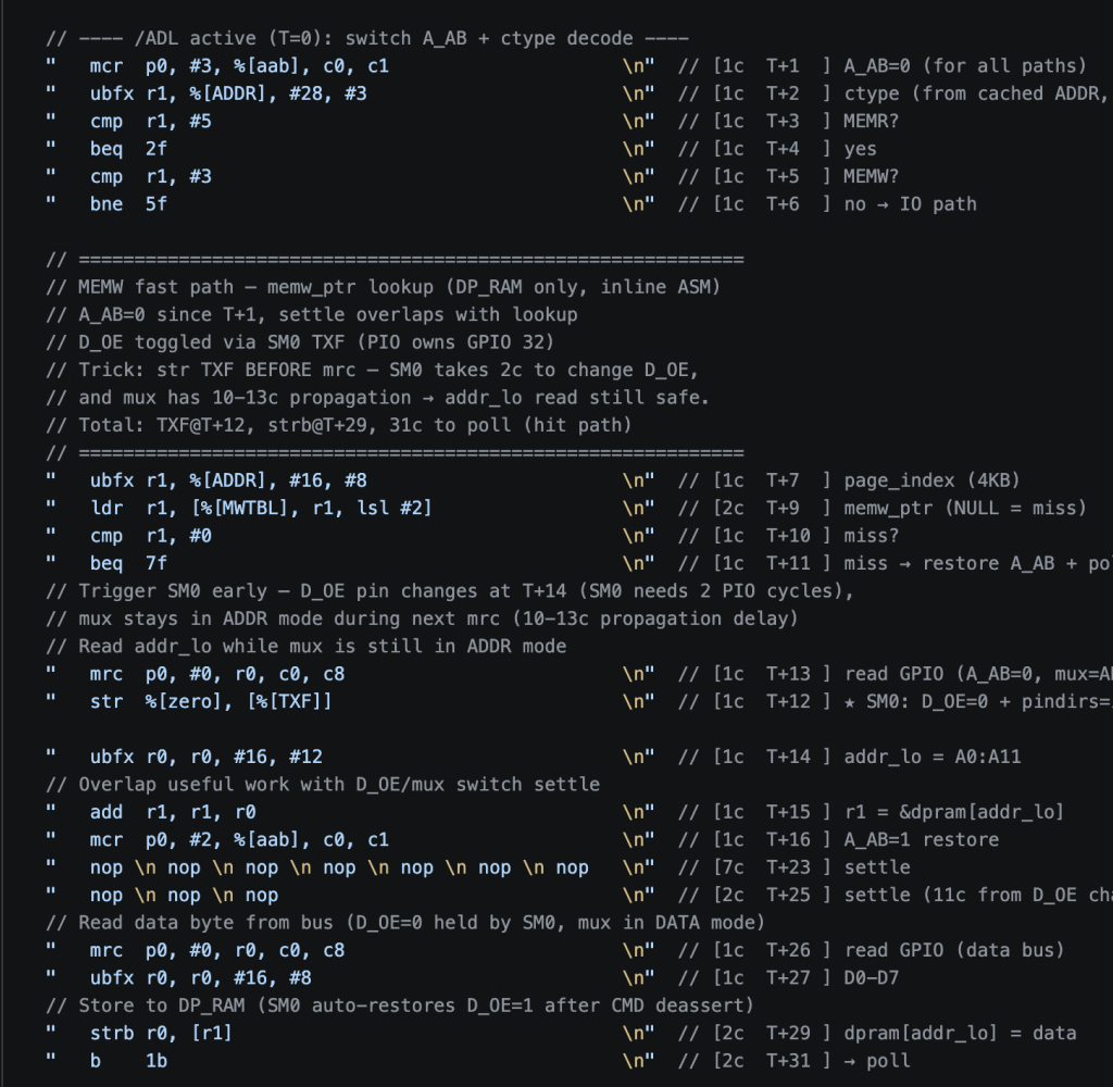
I used the same approach as PicoMEM: write the bus-capture loop in hand-rolled ARM assembly so that every CPU cycle is deterministic and accounted for. C compilers simply don’t give you this level of control over register allocation and instruction ordering.
Everything is gated by /ADL — the active-low Address Latch signal, which indicates that the 24-bit address and the transfer-type signals (S0, S1, M/IO) are stable on the bus.
When /ADL asserts, D_OE is already high and the mux is in address mode, so the upper 12 bits of the address are present on the RP GPIOs and can be sampled immediately. I then drop A_AB from 1 to 0 to bring in the low 12 bits.
This is where it got tricky. You can’t just toggle a GPIO and read the input on the very next instruction — there’s a signal propagation delay in IC between the moment the RP drives its output and the moment the external mux’s outputs actually settle.
On this board:
Data buffer — about 6 to 8 cycles
Address mux — about 4 cycles of propagation delay
Below is the typical timing of a IO cycle on the PS/2 Model 50Z
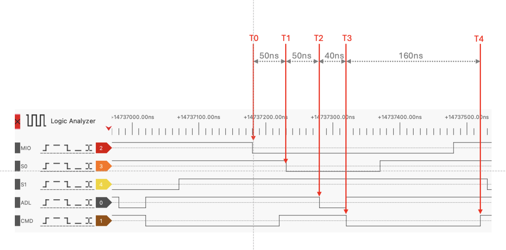
T0 is the start of a new cycle, with MIO falling edge (going LOW) for an IO cycle. It means also that, when Idle MIO is HIGH and it is not possible to capture the start of the MEM (MEMR Read, MEMW Write). At T0, this address (24bits wide) is available on the bus but not stable.
T1 (T+50ns) it is the status line indicating if the cycle is Read or Write
T2 (T0+100ns) is the /ADL signal, for Address Latch, it indicates that the 24bit address on the bus is stable and can be latched by the slave card.
T3 (T0+140ns) is the /CMD signal, used to have the data on the bus read or write. This signal stays valid for 160ns on a typical IO cycle (300ns)
And this is exactly the same for a MEM cycle but with shorter delay between MIO and S0/S1 (10ns) and also a shorter duration of CMD (90ns)
Given that timing, you would consider starting processing right after T1 to maximize the remaining timeframe to execute all the operations before the rising edge of /CMD (T4 end of the cycle). I tried, and it was working pretty well (sometimes) for IO and almost never for MEM cycles.
One of the many particularity of the MCA bus is the ghost cycle, or abandoned cycle, it is cycle without /ADL assertion or /CMD assertion. It happens for 2 reasons, first reason is MEM 8Kb cache on 386 SLC cycle not showing on the MCA Bus, and second reason is the DRAM Refresh cycle without ADL (buried on page 100 of the IBM specifications). It means that the slave (WonderMCA) can not poll a combination of signal between /MIO,S0,S1 for IO and something else for MEM cycle (keep it mind that we have a very tight number of RP2350B cycles to do everything).
Following the Snark Barker card implementation, and the MCA guide from Eric, the only signal that is reliable to trigger a valid cycle is /ADL.
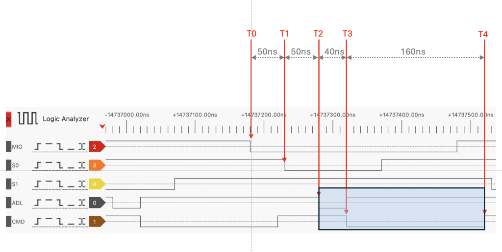
In light blue the exploitation window for the RP2350 to process a MCA bus Cycle and this is 200ns for an IO and 140ns for a MEM cycles.
On top of this, there is signal propagation delay… My nightmare. In theory, you would argue that we are able to capture immediately a signal and also put data signal immediately on the MCA Bus but unfortunately this is not the case.
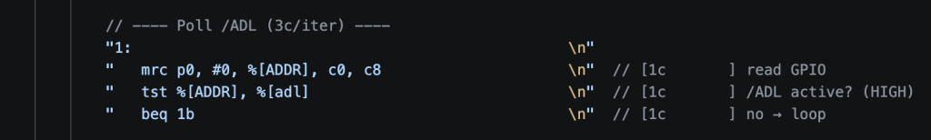
The following code bloc, is a 3 cycles instruction to capture the /ADL signal, at 150 Mhz it would take 3×6,6ns max, in reality electrical propagation is taking 18ns on top of CPU processing.
Then, because we never have enough GPIO on the RP2350, multiplexing is used to capture the 24 bit address lines signal in two passes:
- A_AB HIGH means capture 12 High Address bits,
- A_AB LOW means capture 12 Low Address bits,
The propagation delay of the A_AB multiplexer is another 20ns,
And the last topic is the data buffer propagation delay that is also a 26ns delay.
In summary, over a 200ns cycle you have roughly 60ns spent on electrical signal propagation. My last weeks evening game was to find a way to have this propagation masked with other CPU operations and to fit all conditions in a 140 ns timeframe…
I tried so many scenarios, and hours of debugging…
- Poll at T1, with Max on Addr Low for IO, then switching, with condition on /ADL
- Poll at T2, with Mux on Addr High for MEM, then swithcing
Every time, either MEM was working and not IO and vis & versa.
Channel Ready – down the rabbit hole
While reading this post, you can ask yourself why I do not use the famous CHRDY signal ! The CHRDY stands for Channel Ready signal, and it is used to extend the duration of a cycle while /CHRDY is LOW. I tried but I failed after so many attempts.
Depending on the model (generation) of PS/2, the bus controller is not the same and the signal timing is also not exactly the same… CHRDY is not like the ISA Bus where the bus is on pause when you start asserting the IOCHRDY signal. On the PS/2, the timing is even more complex.
According to the PS/2 specifications, CHRDY need to be asserted a maximum of 60ns after T0 !!! so it means that if you start your cycle with T1 trigger and you have 20ns propagation delay you almost miss every time the CHRDY window and the MCA Bus cycle is never extended… this is the Theory, after doing multiple tests, the behavior is not the same for every MCA Bus controller.
| PS/2 Model | Strict CHRDY 60ns after T0 | CHRDY before rising edge of /ADL |
| 8550Z | X | |
| 8555 | X | |
| 8556 | X | |
| 8557 | X | |
| 8560 | X | |
| P70 | X |
To sort this out, I even tried to trigger chrdy for every cycle (before addr decoding) and if needed to deassert CHRDY on not in scope address. But of course, for some internal PS/2 Bus reasons it was freezing the CPU.
At this stage, I was able to get the MEM (MEMR / MEMW) to execute in an effective 140ns timeframe, but for IO it is impossible due to the Sound Card emulation and other device emulated… The average IO cycle duration is above 400ns…
I did the mem path in full ARM assembly code with the new GPIO coprocessor to be really deterministic and not rely on the compiler optmization
I also use a lot of programming trick like tab of point to faster decode the scope of the MCA bus address.
But still IO is not working, and without IO there is no emulation…
CPLD to rescue the project
The only way to sort this, is the CPLD approach,
A CPLD is a small IC with fuse that is able based on signal equation to trigger basic operation (AND, OR, XOR,NOR,…). The good news is that I had on my bench a small AT22V10C-7PX (DIP24 IC), and I decided to give it a try.
7PX means that is signal is produce with a 7ns delay from input to output.
Hopefully, on the first prototype I put almost every MCA signal on pin header, and I was able to bridge the low address bit and MIO,S0,S1,CHRDY to the CPLD.
I was finally working and I was able to do MEMR/MEMW and IOR/IOW with a form of accuracy.
To be continued