A driver that “shouldn’t” work
For most of WonderMCA’s development the chassis matrix looked encouraging. The card came up clean on the IBM PS/2 Model 8550Z, on the 8555, on the 8556, on the 8557. POST passed, the option ROM checksum was correct, the screenpad lit up, the floppy emulator mounted images, the NE2000 tunnelled traffic over W5500. By early May 2026 four 286-class & 386 PS/2 boxes were green across the matrix.
Then I plugged the same card into a Model 8570 — the 25 MHz 386DX desktop — and got:
D0000 114
POST 114. The chassis BIOS had scanned for option ROMs in the C000–DFFF region, found WonderMCA’s 0x55 0xAA signature at segment D000, summed the declared 16 KB, and the modulo-256 result wasn’t zero. From the chassis’s point of view the option ROM was corrupt.
But it wasn’t corrupt. The 16 KB ROM image is built by rom_checksum.py script which deliberately picks the last byte so the sum modulo 256 lands on zero. The same image worked perfectly on every 286 chassis and other 386 (like the 56 or 57). Same .uf2 file, same RP2350, same CPLD revision. Just a different chassis.
The same image then failed identically on the gas-plasma Model P70. And on the Model 8580.
What all three machines have in common: they’re 386-class. But it seems that the bus is different
So here we were. A card that boots reliably on every 286 PS/2 we own, and crashes the option-ROM checksum on every 386 PS/2 we own. The MCA bus protocol is the same. The IBM HITRA02 timing windows are the same. There was no obvious reason for it not to work.
That’s the worst kind of bug to hunt.
The first wave of hypotheses
Naturally I started with the obvious. The 386 PS/2s have a faster bus (16 MHz vs. 12 MHz typical for the 286 boxes) and a 32-bit data path that decomposes into byte sub-cycles when talking to 8-bit MCA cards like ours. So timing was the prime suspect.
I drew up five hypotheses in the working log:
- Data-hold violation — maybe the RP2350 firmware releases the data bus drivers right at the same edge that the 386 latches the read value, and our CHRDY release ends the cycle a few ns too early for the faster bus.
- Data-setup violation — the mirror image: CHRDY goes high while our data bus is still slewing.
- CHRDY asserted too late — the chassis might have started its default fast-cycle termination before we got our hand up to say “wait”.
- CHRDY coupling — capacitive crosstalk between CHRDY and an adjacent MCA control trace.
- The chassis reads more than 16 KB — different length-byte interpretation, summing past where our zero-correction byte sits.
Using assembly code, I have built a suite of convenient tools to help debug what is happening on the chassis. Two of these tools are a memory fill & dump tool using a prefix
c:\wmfill.com D4 FF AA # Fill the location of D4000 with 0xAA value for 256 Bytes
c:\wmread.com D4 FF # Dump the content of D4000 for FF number of Bytes 256
The above command tool fill and read 256 Bytes at location starting at D4000 and output it on the PS/2 screen. The D4000 is the memory location that is shared between the chassis and the WonderMCA, in a nutshells the RP2350 can write to a memory location and this location is also mapped to the MEMR / MEMW.
The output should be on working MEMR and MEMW working chassis
0xAA 0xAA 0xAA 0xAA 0xAA 0xAA 0xAA 0xAA 0xAA 0xAA 0xAA 0xAA 0xAA 0xAA 0xAA 0xAA 0xAA 0xAA 0xAA 0xAA But on P70, 8580, and 8570 the output was:
0xFF 0xFF 0xAA 0xAA 0xFF 0xFF 0xAA 0xAA 0xFF 0xFF 0xAA 0xAA 0xFF 0xFF 0xAA 0xAA ... Every two bytes the chassis was reading or writing free floating values (FF is most of the time free floating bus). My first reaction was to consider the BUS to be in 32Bit data bus (the WonderMCA in rev 1 is a 8 Bit data bus). But this makes still no sense as consecutive 2 values are not even 16 bits issues.
There was also a strong piece of bench evidence: if I physically disconnected the CHRDY line at the CPLD pin, the 8570 booted. No POST 114. The option ROM read through cleanly and PMBIOS init ran. But in that case the IOW and IOR were not working (CHRDY is needed especially for the IO path).
That ruled out hypothesis 5 (you wouldn’t fix a length mismatch by removing CHRDY) and pointed hard at something CHRDY-related.
What followed was three days of building diagnostic tools (the iostress and iotest2 programs in WonderMCA/x86tools/), capturing traces on a DSLogic, and staring at oscilloscope waveforms wondering why the 286 boxes were so forgiving.
The bench evidence didn’t match any of my hypotheses
iostress was the breakthrough tool, not the breakthrough itself. It hammers a known I/O port with a pattern (FIXED, WALK1, WALK0, COUNTER, RANDOM, FAST, SLOW) and reports the pass rate. On the 8570:
FIXED   pass 3.5%   fail signature: got=0xFF on every failure
WALK1   pass 4.1%   got=0xFF
WALK0   pass 3.8%   got=0xFF
COUNTER pass 3.4%   got=0xFF
On the 8555 (286 control chassis): 100% across the board.
That 0xFF on every failure is what cracked it open. A failing read wasn’t returning wrong data — it was returning floating bus. 0xFF is what you get on the PS/2 data bus when nothing is actively driving it. So either we weren’t driving when we should have been, or we stopped driving before the chassis sampled.
But the IOR firmware path — handle_ior in wm_mca_rp2350_v10.h — was conservative. It set up the data on the bus, asserted CHRDY , and then waited for /CMD to go high before releasing CHRDY and turning off our data drivers. /CMD high = end of cycle = chassis has latched data and moved on. Standard MCA discipline.
So if we were releasing the bus early, something was making us think /CMD had gone high when it hadn’t.
The MADE24 detour
Here’s where I went down a rabbit hole that, in hindsight, was the fastest path to the answer.
The WonderMCA PCB doesn’t connect /CMD directly to the RP2350. The signal comes from the MCA edge connector and feeds a chain of glue chips on the card: a 74LVC04 inverter, then a 74LVC08 AND-gate. The AND-gate has /CMD as one input and MADE24 (Memory ADdress Enable 24, a 386-introduced signal for 32-bit address-bus extension) as the other.
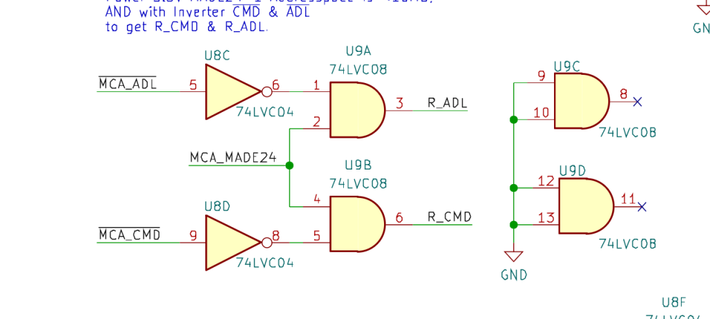
Why? Because on early WM-series prototypes there was a desire to gate /CMD detection on whether the high address bits were valid — a defensive belt-and-suspenders for memory-cycle decoding. The output of that AND-gate fed RP2350 GPIO 15, which the firmware called PIN_R_CMD.
On 286 chassis, MADE24 is driven high and stays high for the duration of every MCA cycle. The AND-gate is essentially a no-op: GPIO 15 mirrors /CMD perfectly. Everything works.
On a 386 PS/2 chassis, MADE24 behaves differently.
The 386 BIU has a 32-bit data path. When it does a read from an 8-bit MCA card, it issues a 32-bit cycle that gets decomposed into four 8-bit sub-cycles by the chassis’s bus controller. MADE24 toggles between those sub-cycles, dropping LOW for tens of nanoseconds during the cycle, then back HIGH for the next sub-cycle.
For an AND-gate with /CMD on one input and MADE24 on the other, MADE24 going LOW pulls the output LOW even though /CMD is still LOW (asserted, cycle in progress). The 8-bit MCA card has no business caring about MADE24 — but the AND-gate cares.
Our firmware sees the AND-gate output go HIGH (because the inverter flipped the LOW), reads that as “/CMD just went HIGH”, concludes the cycle is over, and:
- Releases RP_REL → CPLD releases CHRDY
- Turns off the data bus drivers
The chassis CPU, which is not actually done with the cycle yet, keeps sampling the bus a few ns later and reads… 0xFF. Floating bus.
That’s why every failure had got=0xFF. That’s why removing CHRDY “fixed” it — without CHRDY assertion the chassis never stretched the cycle, so it didn’t matter that we released early. That’s why 286 boxes were fine — MADE24 stays solid on them.
This is you can see unless you trust your intuition and you keep an eye of the MCA raw signal and what is coming to the RP.
The fix: one patch wire + two lines of C
The fix was actually a two-step thing — half copper, half code.
The WonderMCA WM10 PCB as fabricated only had one /CMD path: from the MCA edge connector, through the 74LVC04 inverter, into the 74LVC08 AND-gate (the one with MADE24), out to RP2350 GPIO 15. There was no clean /CMD path on the board. Everything that wanted to look at /CMD had to look at the AND-gate output — which, as we’d just discovered, lied on 386 chassis.
Out came the soldering iron.
I tacked a patch wire from the clean side of the /CMD trace (the 74LVC04 inverter output, before it enters the AND-gate) directly to RP2350 GPIO 47 on the high bank. A thin enamelled wire, 30 AWG, maybe 30 mm long, soldered under a microscope between two otherwise-unused pads. That gave the RP2350 a second view of /CMD — the same signal as GPIO 15, but on a path that bypasses the AND-gate entirely and therefore can’t be tricked by MADE24 toggling.
I named that new pin PIN_R_CMD_HI in the firmware. The schematic comment that ended up next to it for a while (“/CMD mirror — same signal as GPIO 15”) was misleading and got rewritten later: the two pins look at the same logical /CMD, but the GPIO 15 view is contaminated by MADE24 on 386 chassis and the GPIO 47 view is not.
Then the two-line firmware change:
<em>// Before — sampling the AND-gate output, glitches on 386:</em>
while (!(gpioc_lo_in_get() & cmd_mask)) {
    tight_loop_contents();
}

<em>// After — sampling the clean /CMD via GPIO 47 (the patch-wire path):</em>
const uint32_t cmd_hi_mask = 1u << (PIN_R_CMD_HI - 32);
while (!(gpioc_hi_in_get() & cmd_hi_mask)) {
    tight_loop_contents();
}
No CPLD revision. The PIO state machine that watches for the start of a bus cycle wasn’t even looking at /CMD (it triggers on /ADL, which is clean), so it didn’t need touching. Only the C-side post-data /CMD wait was sampling the bad pin. Switching it to GPIO 47 closed the loop.
I flashed the firmware, plugged the patched 8570 back in, and:
iostress 320
FIXED   pass 100.0%
WALK1   pass 100.0%
WALK0   pass 100.0%
COUNTER pass 100.0%
RANDOM  pass 100.0%
FAST    pass 100.0%
SLOW    pass 100.0%
POST 114 was gone. The option ROM checksummed cleanly. PMBIOS init ran. The PicoMEM screenpad woke up. Booting DOS from the emulated HDD worked. The 286 boxes still passed 100% — no regression.
Plot twist: IOW was affected too
Here’s where the bug surprised me a second time.
The bench evidence I had focused on was all about reads — iostress hammered I/O reads, POST 114 was a read checksum failure. So I had patched handle_ior (the IOR handler) in the firmware and called it done.
But then a separate test started misbehaving. The PCCMD protocol — the WonderMCA-to-Pico command channel that uses an I/O range to push mini-RPCs — was timing out on the 8570 even after the IOR fix. The serial log showed:
PC_MemCopyW_512b: Timeout 20ms/100ms
PCCMD: pcs=00 pms=00 cmd=00 src=1
PCCMD uses writes (OUT instructions) from the PMBIOS option ROM to push command headers into a small register set, then reads back the result. The 8570 was successfully reading (because I’d fixed IOR), but the writes were getting lost.
The penny dropped: handle_iow had the exact same code pattern as handle_ior — sample GPIO 15 to detect /CMD going HIGH, then release SFDBK. Same AND-gate, same MADE24 toggle, same false-positive.
On a write the symptom is sneakier. The chassis is the one driving the data bus. When we release SFDBK early, the chassis is still actively driving the data — so we don’t see “0xFF on every failure” like we did with reads. Instead the write appears to complete but our PIO state machine’s data-capture timing slides into a window where the GPIO snapshot might or might not catch the right byte, depending on what the chassis CPU is doing nanoseconds later. The 8570 cold-boot crash during MEM_Test_ROM and the MBR read timeout via PC_MemCopyW_512b were the same bug as POST 114, just on the IOW path.
One more two-line change to handle_iow to switch its post-data wait from cmd_mask to cmd_hi_mask. Built, flashed, tested. The cold- boot crash disappeared. The PCCMD timeouts vanished. The MBR read worked. The 8570 finally booted DOS reliably end-to-end. The 8580 followed. The P70 followed.
What the PCB is going to do about it
The patch wire works. Every WM10 board in field testing has now had the same 30 mm of enamelled wire tacked between the 74LVC04 output and RP2350 GPIO 47, and every one of them boots cleanly on every chassis I’ve thrown at them.
But a patch wire is a temporary solution. It’s fragile (one accidental tug and it’s gone), it’s slow to apply (microscope work, careful soldering, easy to bridge to a neighbour), and it screams “prototype” to anyone opening the case.
The next PCB revision (WM11) will fix it properly in copper. Two small changes to the schematic:
- Remove the 74LVC08 AND-gate from the /CMD path. There was never an MCA-bus reason to gate /CMD detection on MADE24 — 8-bit MCA cards have no business looking at the 32-bit address extension. The AND-gate was a defensive holdover from an early prototype that nobody ever validated against a 386 chassis.
- Route /CMD directly to RP2350 GPIO 47 (what the patch wire currently does, in copper instead of hand-soldered).
GPIO 15 becomes free for another signal. The 74LVC08 footprint can be depopulated or removed. The firmware doesn’t change — PIN_R_CMD_HI is already pointing at the right pin and the wait loops are already sampling it.
Until then, the patch wire is the rule: any WM10 board that’s going to be used on a 386 PS/2 needs the modification before it’ll boot reliably.
Lessons
- The chassis matrix is the spec. The HITRA02 timing windows describe what the bus can look like. What it actually looks like varies by chassis generation in ways the spec doesn’t enumerate. You can’t validate a card against the 286 PS/2s and assume the 386 PS/2s behave the same way — and Big Blue isn’t around to tell you what’s different.
- The bug always shows up on the path you didn’t look at first. I had spent days on the IOR side because the symptoms presented as read failures. The IOW side had the same code, the same bug, the same root cause — but the symptom on IOW was subtle enough that I didn’t notice until a completely different test surfaced it. Once you find a code pattern that’s wrong, search the codebase for that exact pattern and fix every instance.
0xFF on every failureis a tell. A bus that should be driven but returns all-ones is screaming at you: I’m reading from the floating bus, somebody isn’t driving when they should be. Once you recognize that signature, the problem space collapses from “what could possibly go wrong” to “who released the bus early and why”.- Trust the schematic but verify the timing. The schematic originally treated /CMD as a clean signal once it left the inverter. The 74LVC08 AND-gate downstream was a defensive add that ended up being the bug. “Logically the same signal” is not the same as “electrically the same signal” — two GPIOs sampling the same source through different paths can give you different answers nanoseconds apart.
- A patch wire plus two lines of firmware beats waiting for a respin. A PCB revision is weeks of CAD + fab + assembly + bring-up. A patch wire is ten minutes under the microscope. The WM11 board will clean this up in copper — no AND-gate, /CMD goes straight to GPIO 47 — but the WM10 fleet works today with one bodge wire and two lines of C, and that’s what gets the testers booting their 386s tonight instead of in October.
The 8570, the 8580, and the P70 now all boot cleanly with the same firmware that runs on the 8550Z and 8556. The chassis matrix is green for the first time since this project started.
Next bug please