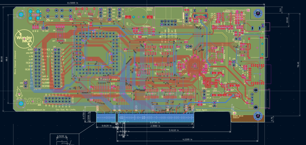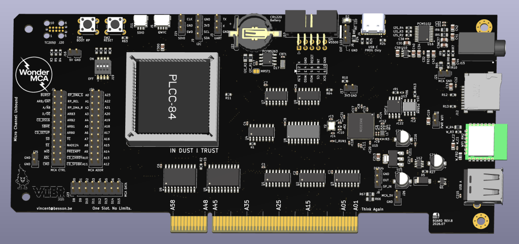
On this project, I have so far made 2 prototype versions of the PCB, the REV2 and the REV5. The REV2 was a real draft with no CPLD to manage the MCA bus constraints, and it was a good base with all the MCA signals available on PIN Header to prototype what was supposed to be a solid version (REV5). The PCB Revision 5 is using an ATF1508 in PLCC84 format, and was supposed to be working smoothly but it was clearly not the case.
I made several mistakes on the Rev5:
- JLCPCB 10K resistors wrong 0603 reference giving 1K8 instead of 10K,
- TC2050 CPLD upload connector missing +5V from the board (as buried in the programmer reference document)
- Wrong footprint on the LDO (Power supply) of the DAC circuit,
All these should be fix with the REV8 of the board… But it is not the main issue of the REV5…
The main issue with the REV5 is the USB instability, or USB PHY issue. The symptoms are very uncommon:
- RP2350 firmware upload impossible when powered with MCA Bus,
- Boot from USB Floppy image crashing the WonderMCA BIOS with TinyUSB panic error on the console,
- Same panic errors when using USB network controller.
and for the record the REV2 was not facing the same type of strange behaviors…
Of course you would argue that I just have to compare the PCB from REV2 to REV5 and identify the gap… but the tricky part is that there is no difference (or very small difference) between the 2. I asked for help on this and Polpo (the Father of the PicoGus) confirmed that the USB on the RP2350 is forgiving a lot.
I can not decide myself to fabric a new PCB without addressing this very specific issue, and I think I found the source of the problem. On the fun part, following an advice from a friend who told me “You should ask Claude…”, I asked Claude 100x and each time I received a different answer and of course not the real reason why… there is still room for human to solve poor defined problems.
I think I found the issue and I was from the beginning looking at the wrong place. My initial theory was a cross talk between the QSPI (Flash and PSRAM) and the USB.
The first image is the REV2 routing zone around PSRAM and USB
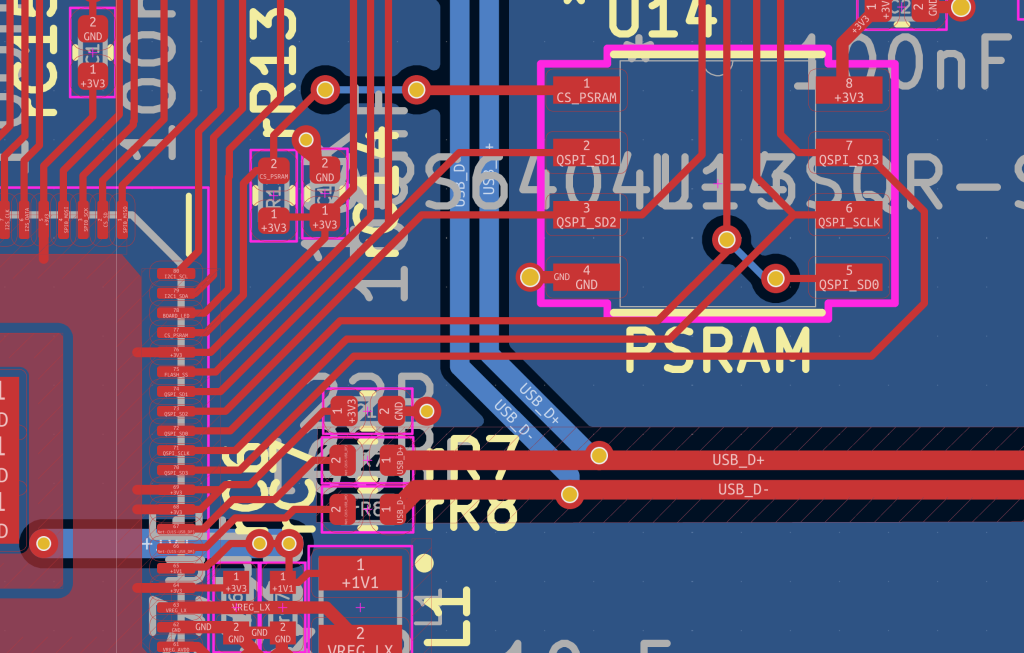
As you can see there is room between the USB_D+ and the QSPI_D3 and QSPI_SCLK
The next image is the REV5 same routing zone :
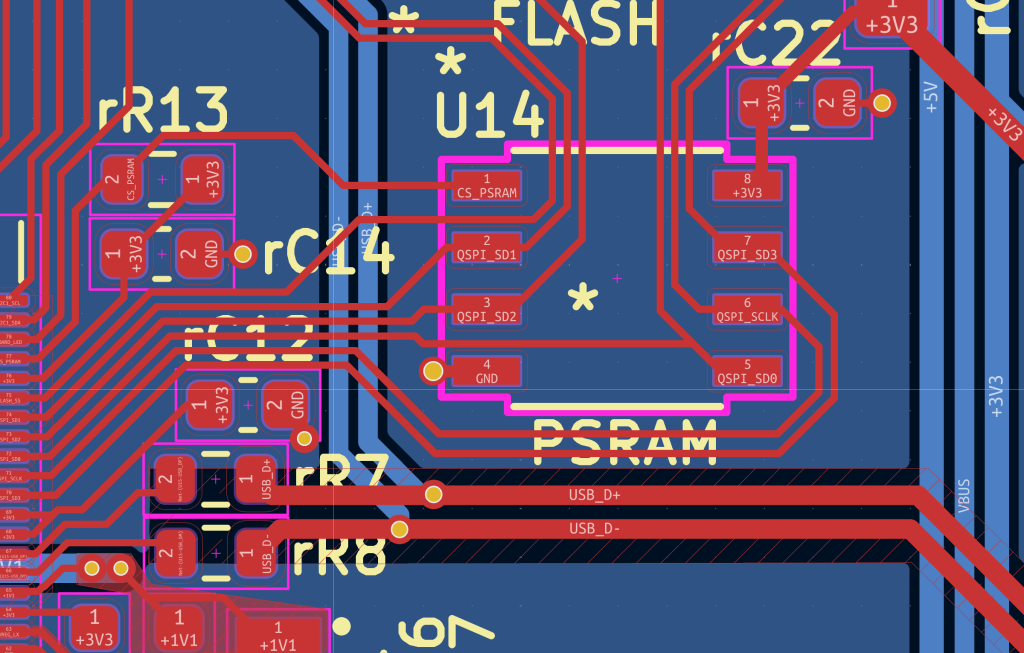
As you can see, the gap between USB_D+ and QSPI_SD3 is clearly not helping… and my initial suspicion was a cross talk generating on the PSRAM side corruption and the same on USB PHY interface.
However, I thought that this simple explanation was not enough… and the fact that the USB issue was happening only when the RP2350 Core1 was under MCA BUS load was clearly pointing to something else but what ? Of course my design around PSRAM is really ugly and not right but it was not the main reason (I think).
Between the REV2 and the REV5, I have changed the buffer from the MCA Bus to the RP2350 (5V to 3V 3 state output) to have more output pin, and I have also change the RP2350 caps and resistors (from 0402 to 0603) footprints and routing (bad move).
When the bus is quiet I do not have any issue, as soon as I have MEMR/MEMW I start getting USB PHY corruption, and yesterday evening I found something (obvious)…
Here is the REV2 routing on the left of the RP2350, and this version of the PCB is working:
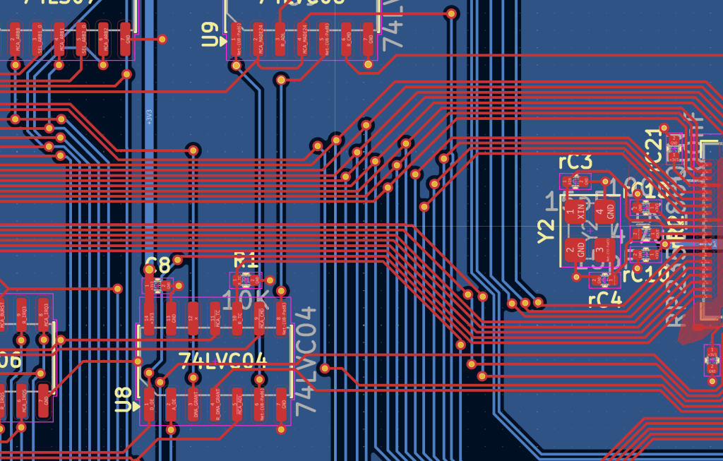
This is the part of the REV5 routing around the same zone:
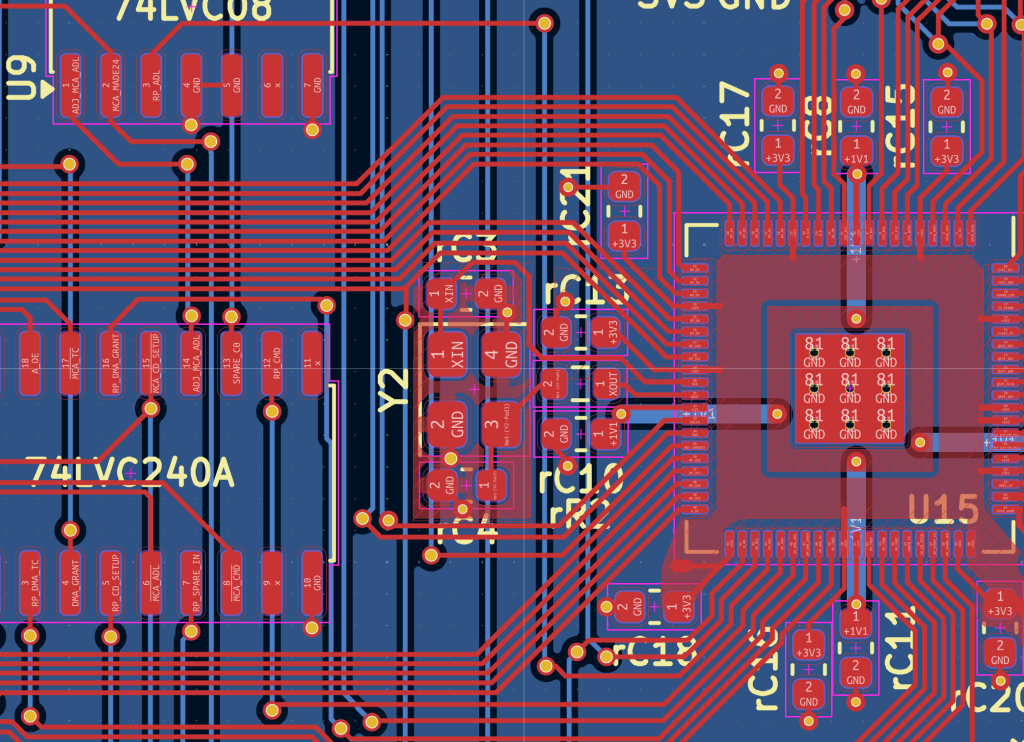
The difference between the 2 is the /ADL signal from the MCA bus going below the RP2350 crystal oscillator and caps… (the blue lines below XIN). On this 2 layer board, my suspicion is an EMC crosstalk between ADL and the clock signal to the RP2350 that would explain the USB clock issue and as well the Flash RxDelay and ClockDIV poor performance.
This zone is really sensitive and especially on a 2 layer board with no solid GND layer, nothing should be below the crystal and the RP2350… and I did it 😉
If it is the case it is a good learning, the hard way, but still it gave me the opportunity to address many other topics (crosstalk CLK optimization, USB impedance calculation, GND plate construction,…)
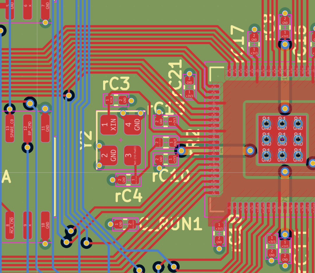
Based on the advice of FreddyV (Picomem father), I moved the design the a 4 layer PCB with In1 being GND and In2 being +VCC. Of course it has a manufacturing cost but my objective is to create the best version of the WonderMCA and manufacturing as well as BOM constraint are not really considered yet.
On the REV8 this is the new crystal zone:
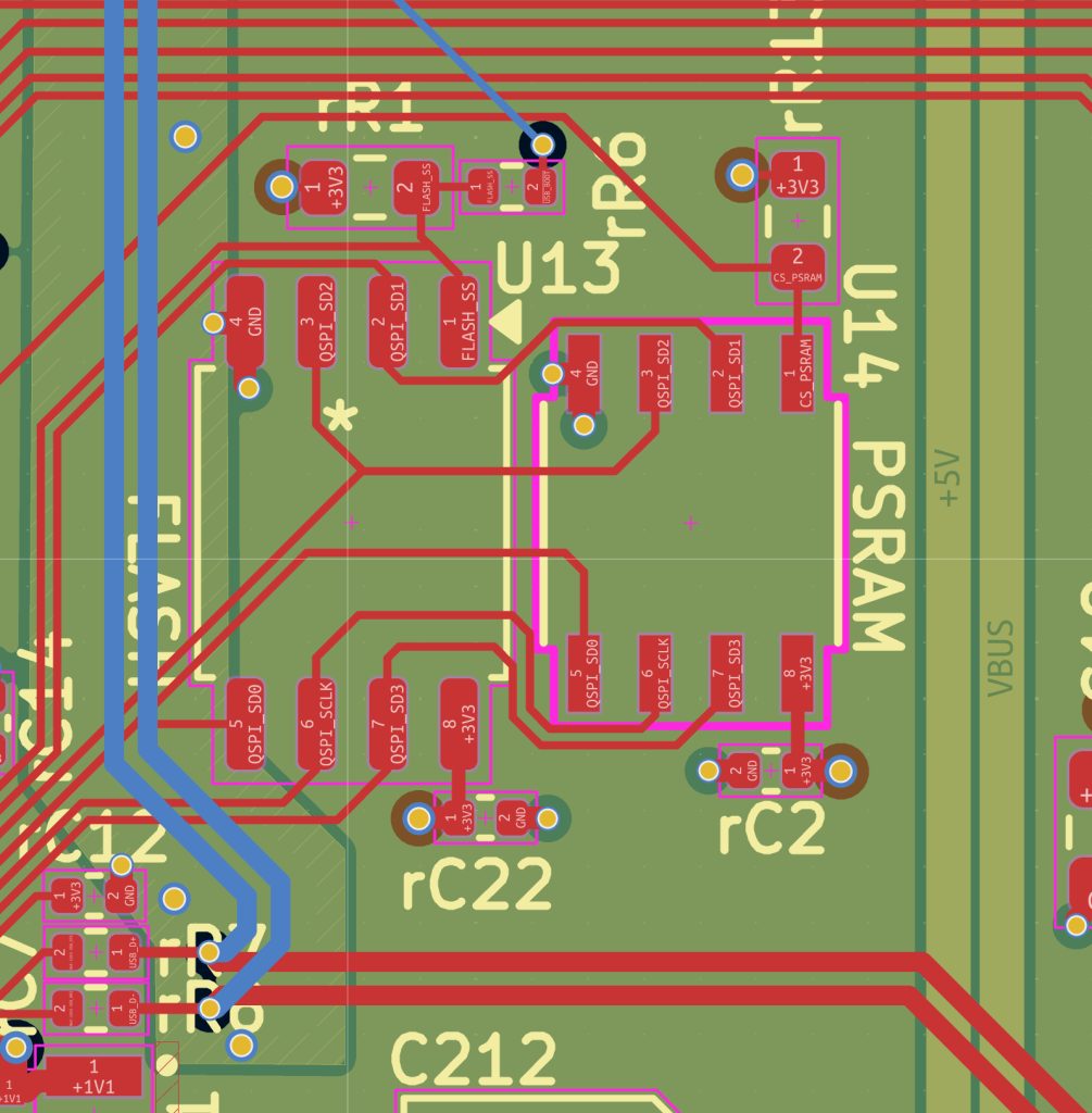
I have also rerouted the USB side with a clean PSRAM / FLASH zone and 90 Ohm USB impedance
I also change the DAC analogic GND zone following PCM5102 best practices:
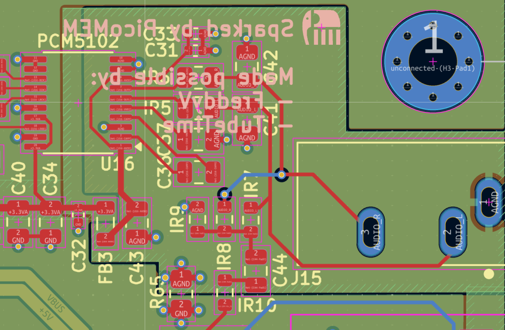
The last major change on the REV9 is have the MCA OSC (Clock signal) to be routed to the CPLD,
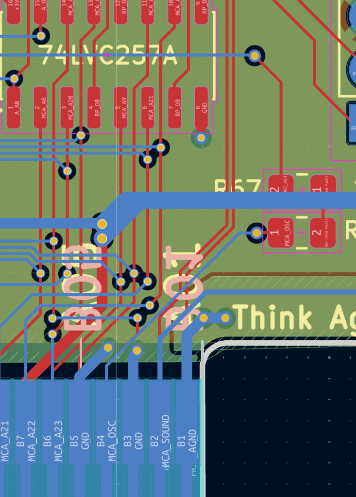
Why MCA_OSC ? MCA_OSC is the clock signal (14.31818 MHz clock) from the B4 Edge connector (Pin 4 B side) providing the chassis clock signal. It is not a signal aligned with the MCA MEMR /MEMW or IO, just a clock signal from the BUS. I want to use this signal to build a CHRDY counter on the CPLD and to avoid the nice DMA timeout (famous NMI error 113). This way the CPLD will use macrocells to count the number of pulse from the CHRDY assertion and force the release if the RP2350 is not asserting the REL signal. I do not know if it will work but now I have this signal that was missing on the previous revision. I have a 0R resistor to be able to remove the signal to the CPLD and also a 68R resistor to avoid signal reflection to the BUS (and everything in 0805 footprint, easy to be changed and resolder).
This is where I am so far, the REV8 is finally ready to be sent to JLCPCB, crossing fingers to be the right version 😉